WHY IS SEM IMAGING USED TO STUDY NANOFIBRES?

SEM imaging is an ideal tool to check the homogeneity and diameter of nanofibres. SEM manufacturers have developed specific software applications for a fully automatic fibre diameter distribution measurement. Nanofibres are also used in air filtration applications for antibacterial and nanoparticle applications. SEM imaging (eventually combined with EDS chemical microanalysis techniques) to check the filter efficiency or to analyse the material that is captured on the filter. Most natural and synthetic polymers are good thermal and electrical insulators. This means that when the nanofibres or the materials that are commercially developed from nanofibres are scanned by the electron beam in a microscope, sample charging with often occur.

CLICK HERE to download the full application note.
For further information, application support, demo or quotation requests please contact us on 01582 764334 or click here to email.
Lambda Photometrics is the leading UK Distributor of Characterisation, Measurement and Analysis solutions with particular expertise in Instrumentation, Laser and Light based products, Optics, Electro-optic Testing, Spectroscopy, Machine Vision, Optical Metrology, Fibre Optics, Microscopy and Anti-vibration tables & custom solutions.
-
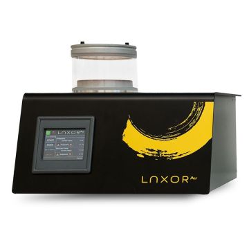
LUXOR Gold Coater
The LUXORAu is an advanced, fully automated sputtering device that applies a fine grain gold coating from 1 to 100 nm thickness. This allows you to get the very best SEM imaging quality from your samples.
LUXOR’s unique A² technology generates a gold plasma and sprays it in a controlled and accurate manner, resulting in an extremely uniform, thin and homogeneous gold layer.
The LUXORAu is also renowned for its ease of use and quick, hassle-free operation.
-
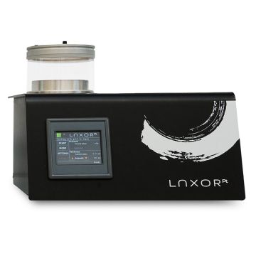
LUXOR Platinum Coater
The LUXORPt is a highly innovative, fully automated sputtering device which applies a fine grain platinum or gold coating from 1 to 100 nm thickness.
LUXOR’s unique A² technology assures that the gold or platinum is sprayed in a highly controlled and precise manner, resulting in an extremely uniform, thin and homogeneous coating.
This allows your scanning electron microscope to show the best possible image quality.
-
LUXOR Sample Holder for Mounted/Embedded Samples
The LUXOR sample holder for mounted/embedded samples can hold all types of samples that are mounted or embedded into resins with diameter ranging from 25 mm to 40 mm and height from 10 mm to 50 mm.
-

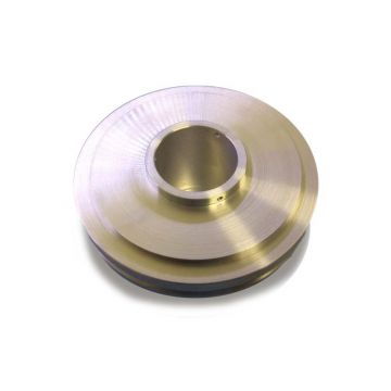
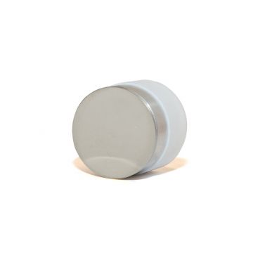
LUXOR Gold Target
Gold target Ø 30 mm, thickness 100 µm (99.999% purity) for use with both LUXORAu and LUXORPt
-
LUXOR Platinum Target
Platinum target Ø 30 mm, thickness 100 µm (99,999% purity) for use with LUXORPt
-