


The growing diversity in the used materials in semiconductor packaging provides challenges for achieving good interconnection. Particularly the very soft substrates, such as paper and polymers, and very hard, such as silicon carbide, offer unique challenges to wire-bonding or formation of vertical interconnects. Complementary technologies are therefore needed. Here, a method to direct-write metal tracks on the top and sides of dies is demonstrated. It is based on a spark ablation aerosol printing process entirely performed at room temperature and without any applied force. Therefore, it is suitable for use on soft or temperature-sensitive substrates. The printed metal lines consist of pure Au nanoparticles, without surfactants or contaminants, and do not require any further curing, cleaning, or other processing. The process is demonstrated on Si dies and paper, but is theoretically applicable on a wide variety of substrate materials. It can provide an alternative method to create interconnects or vias on soft materials, temperature sensitive materials, irregularly shaped materials, or curved surfaces.
DOI: 10.23919/EMPC53418.2021.9585005
Click HERE to read the full paper.
To speak with one of our Sales & Applications Engineers please call 01582 764334 or click here to email.
Lambda Photometrics is the leading UK Distributor of Characterisation, Measurement and Analysis solutions with particular expertise in Instrumentation, Laser & Light based products, Optics, Electro-optic Testing, Spectroscopy, Machine Vision, Optical Metrology, Fibre Optics, Microscopy and Anti-vibration tables & custom solutions
-

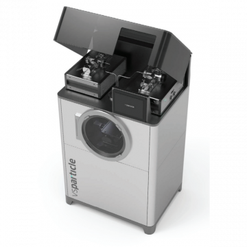
VSPARTICLE VSP-G1 Nanoparticle Generator
A table-top, user-friendly nanoparticle generator that is the basis of all VSPARTICLE products. With the VSP-G1, a stable and clean flow of well-defined pure nanoparticles can be generated, without the use of precursors and surfactants. Producing the desired particles becomes as easy as pushing a button.
-
VSPARTICLE VSP-P1 Nanoprinter
Local deposition of nanoporous thin-films. When connected to the output of the VSP-G1, the VSP-P1 enables you to print inorganic nanostructured materials with novel properties. The material is built-up of sub 20nm pure particles, and can be printed in patterns locally on any type of substrate.