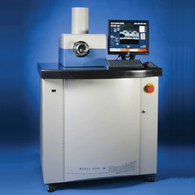
Fischione Model 1063 WaferMill™ Ion Beam Delayering Solution

- Selected-area milling on full 300 mm wafers
- Top-down delayering
- Expose multiple device layers and structures
- For use in multiple areas of a semiconductor fabrication facility:
– Research and development
– Process control
– Yield enhancement
– Failure analysis
CD-SEM specimen preparation
Critical dimensions (CDs) of microscopic patterned wafer features are measured by scanning electron microscope during the semiconductor manufacturing process. In conventional CD-SEM specimen preparation, individual dies are cut from a wafer and then each specimen is prepared by a traditional ion milling system, one specimen at a time.
With the Fischione Model 1063 WaferMill solution, you can delayer multiple pre-selected regions on a full wafer from the top down. The entire process is fully automated; there is no need to manually touch a wafer. The Fischione Model 1063 WaferMill solution supports metrology, including CD-SEM sample preparation.
WaferMill solution components
Equipment front-end module (EFEM). The EFEM receives the front opening unified pod (FOUP) and transfers the specified wafer into the processing chamber. The EFEM contains:
- One FOUP loading station that holds 25 wafers that can be up to 300 mm in diameter.
- Four-axis wafer handling robot with a passive end effector to transfer the wafer from the FOUP into the pre-pump chamber.
- Pre-aligner to initially orient the wafer so that pre-established sites can be ion milled.
Pre-pump chamber. The pre-pump chamber interfaces with the EFEM through a 300 mm gate valve. A dedicated turbomolecular drag pump evacuates the pre-pump chamber.
UV light. The pre-pump chamber includes a dual wave length (253.7 nm and 184.9 nm) ultraviolet (UV) light that cleans the wafer post ion milling before reloading the wafer into the FOUP.
Load lock. The wafer moves from the pre-pump chamber to the process chamber through a second 300 mm gate valve.
Process chamber. The wafer is captured by an electrostatic chuck, which ensures an even milling plane by eliminating any bow in the wafer. The stage translates into the milling position (x and θ), which allows access to any position on the wafer. The turret contains three argon ion sources that provide uniform milling, as well as a rocking assembly (120 ±10°). Rotating the turret normalizes milling and avoids curtaining. A dedicated turbomolecular drag pump maintains the desired chamber pressure.
|
Model 1063 WaferMill™ ion beam delayering solution specifications |
|
|
Applications |
Near-line and in-line |
|
Equipment front-end module (EFEM) |
Manufactured by Brooks Automation; comprises the following: • 300 mm front-opening unified pod (FOUP) loading station that holds up to 25 wafers |
|
|
• Four-axis wafer handling robot with a passive end effector |
|
|
• Pre-aligner that orients the wafer notch based on CD-SEM requirements |
|
|
• Controller unit |
|
Pre-pump chamber |
300 mm VAT valve interface between the EFEM and load lock |
|
UV light |
Dual wave-length ultraviolet (UV) light (253.7 nm and 184.9 nm) mounted within the pre-pump chamber |
|
Load lock |
A 300 mm VAT valve interface between the pre-pump chamber and the process chamber; wafer presence sensors indicate when a wafer is in the load lock |
|
Vacuum system |
Two dedicated turbomolecular pumps; one in pre-pump chamber and one in process chamber |
|
|
Oil-free diaphragm pump to back turbomolecular pumps |
|
|
Pressure monitoring with vacuum gauges |
|
Pneumatic supply |
Load lock and milling chamber: |
|
|
• Process gas: Inert gas (argon) with purity of 99.999% (ultra-high purity); 20 to 30 psi |
|
|
• Control gas: Dry nitrogen; 60 ±5 psi |
|
|
• Load lock vent gas: Clean, dry air (CDA); 20 to 30 psi |
|
|
• Automatic gas control: Three mass flow controllers (one per ion source) |
|
Process chamber |
Linear stage moves the wafer in the x and y direction with 5 μm |
|
|
accuracy |
|
|
Electrostatic chuck: Grips the wafer in place to provide a uniform |
|
|
milling plane by eliminating wafer bow |
|
|
Wafer presence sensors: Indicate when a wafer is in the process |
|
|
chamber |
|
|
Integrated wafer mapping based on KLARF files |
|
|
Ion source assembly: Three ion sources, located 120° apart, at 22.5° |
|
|
from the horizontal plane. |
|
|
• Variable energy (4.0 to 10.0 keV) operation |
|
|
• Beam current density: 10 mA/cm2 |
|
|
• Beam size: 2 mm |
|
|
• Point targeting provides the ability to drive the wafer to any point |
|
|
for processing |
|
|
Turret/rocking assembly: |
|
|
• Can be rocked ± 175° |
|
|
• Angular deviation is ± 5° with a variable step size range of 0.1 to 2° |
|
|
• Rocking speed is 1 rpm. |
|
Automatic |
• By timer |
|
termination |
• By image processing; milling stops when a specified diameter is |
|
|
reached |
|
User interface |
PC-based interface: |
|
|
• Accessible from EFEM and chamber side |
|
|
• Used to control the milling process |
|
|
Operation indicator: Stack light |
|
Optical system |
Optical system for beam process monitoring and image acquisition: |
|
|
• Field of view: |
|
|
– 15 mm (low magnification) |
|
|
– 1.4 mm (high magnification) |
|
|
• Motorized zoom |
|
|
• Motorized focus |
|
EFEM electrical |
• Electrical system: 200-240 VAC, 50/60 Hz, single phase (L1, L2, PE) |
|
requirements |
• System full load current: 20 A |
|
|
• Constant load range 5-14 A, depending on configuration |
|
|
• Overvoltage category II |
|
|
• Jet power distribution unit is supplied with 10,000 AIC circuit |
|
|
breakers; SCCR 10,000 A |
|
|
• House vacuum: < 40 kPa (7 psi) |
|
|
• Vacuum port: 8 mm quick connect |
|
Power |
208-240 VAC 50/60 Hz, 5200 Watts |
|
Warranty |
One year |